Copper Cubic Crystals
Affiliation:
Merlin Circuit Technology Ltd, Heriot-Watt University
Description:
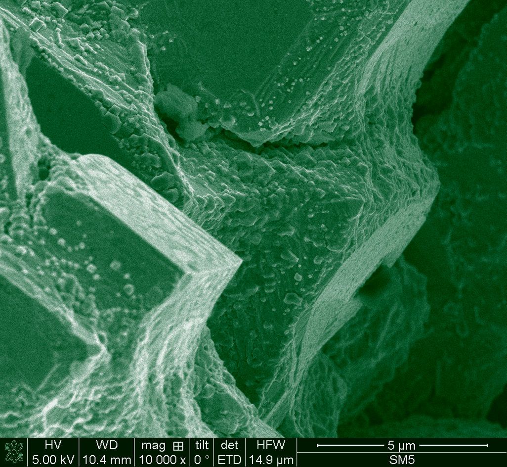
The scanning electron microscope false colour image highlights the surface topography for electroplated copper on top of a printed circuit board (PCB). In this example the deposition has undergone an adverse plating reaction leading to the formation of large copper crystals. The copper crystals are produced in response to an extremely slow deposition rate which is proportional to the electrical current supplied to the PCB. Under the low current conditions the step-growth of individual large crystal facets is favoured which highlight the underlying face-centred-cubic structure of the copper crystal system. The large crystals were possible due to their interrupted deposition during plating. A uniform small grain finish is desired in PCB manufacture and so a cubic plated finish is unwanted due to its sand-paper like quality. Its brittle nature also makes it unsuitable for further PCB manufacture processing. The image highlights that when the electrical current is pushed below a limiting value a poor deposition occurs.
Equipment used:
Scanning Electron Microscope