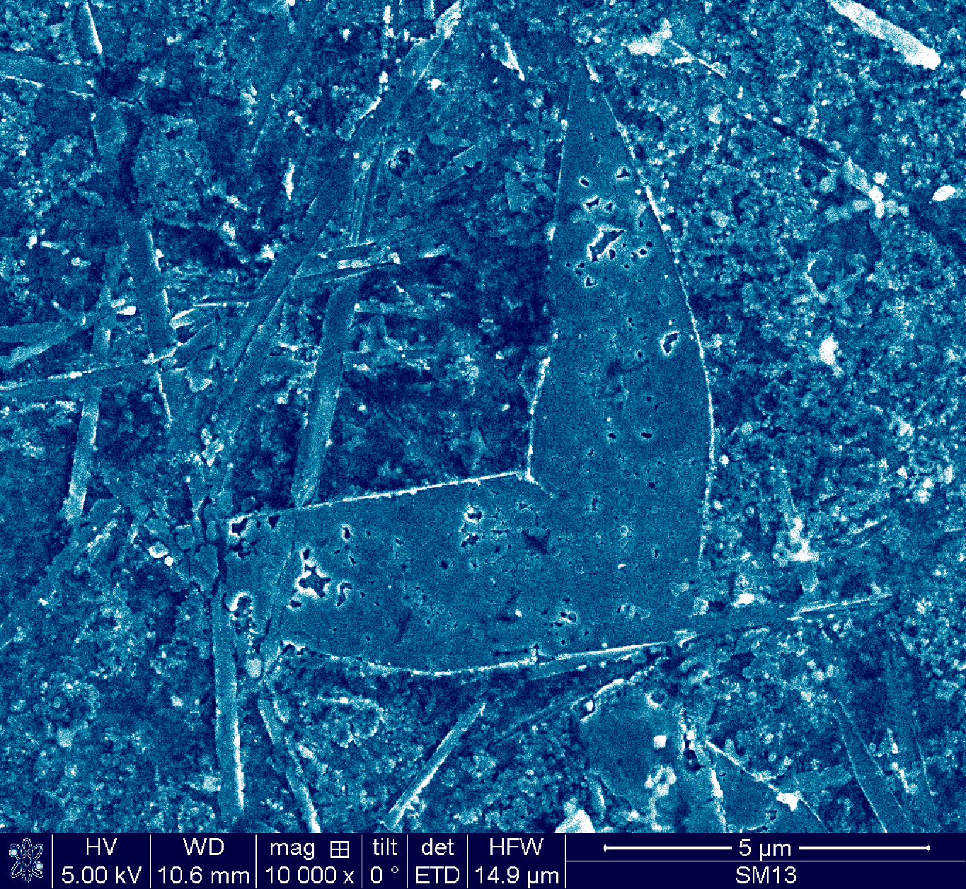
Copper Leaf
Affiliation:
Merlin Circuit Technology Ltd, Heriot-Watt University
Description:
The scanning electron microscope false colour image highlights the surface topography for electroplated copper on top of a printed circuit board (PCB). The leaf-like feature is due to a spiky, filament large crystal growth of copper. Copper spikes are unwanted in PCB manufacture due to their poor uniformity and strength of deposit. A spiky deposition is formed when the crystal growth is fast and the plating chemistry concentration is below a limiting value. The random nature of the crystal orientations is because the deposit was interrupted whilst it was layered and its fast deposition rate due to the high electrical current supplied to the PCB. The mechanism behind a spiky growth is the protruding tips of underlying copper crystals act as electrically isolated features, which under high current settings lead to the increased attraction of the electrical current and thus act as nuclei for the formation of copper spikes. The image highlights that when the plating chemical levels are below a limiting value and the current is high an unwanted copper deposition occurs.
Equipment used:
Scanning Electron Microscope